Most Popular
-
1
Seoul transit pass for travelers to be available starting July

-
2
Controversy rekindled over when to name criminals, suspects

-
3
[Weekender] Pet food makers bet big on ‘recession-free’ pet food market
![[Weekender] Pet food makers bet big on ‘recession-free’ pet food market](//res.heraldm.com/phpwas/restmb_idxmake.php?idx=644&simg=/content/image/2024/05/10/20240510050754_0.jpg&u=20240512145510)
-
4
N. Korea says to deploy new multiple rocket launcher starting this year

-
5
[Drama Tour] Romantic trip to ‘Queen of Tears’ filming spots
![[Drama Tour] Romantic trip to ‘Queen of Tears’ filming spots](//res.heraldm.com/phpwas/restmb_idxmake.php?idx=644&simg=/content/image/2024/05/09/20240509050798_0.jpg&u=20240511190213)


![[Weekender] Pet food makers bet big on ‘recession-free’ pet food market](http://res.heraldm.com/phpwas/restmb_idxmake.php?idx=644&simg=/content/image/2024/05/10/20240510050754_0.jpg&u=20240512145510)

![[Drama Tour] Romantic trip to ‘Queen of Tears’ filming spots](http://res.heraldm.com/phpwas/restmb_idxmake.php?idx=644&simg=/content/image/2024/05/09/20240509050798_0.jpg&u=20240511190213)
-
6
Hybe-Ador CEO conflict gets messier

-
7
Battery makers ramp up efforts to diversify graphite supply chain

-
8
[LLG] Unseen inheritance: Trauma of transnational adoption 'trickles down' to adoptees' children
![[LLG] Unseen inheritance: Trauma of transnational adoption 'trickles down' to adoptees' children](//res.heraldm.com/phpwas/restmb_idxmake.php?idx=644&simg=/content/image/2024/05/12/20240512050141_0.jpg&u=20240512163544)
-
9
‘Monk’ DJ spreading Buddhism goes global

-
10
Prosecutors to summon pastor who allegedly gave Dior bag to first lady


![[LLG] Unseen inheritance: Trauma of transnational adoption 'trickles down' to adoptees' children](http://res.heraldm.com/phpwas/restmb_idxmake.php?idx=644&simg=/content/image/2024/05/12/20240512050141_0.jpg&u=20240512163544)


Samsung chief bolsters ties with Germany’s Zeiss
Lee Jae-yong travels to Europe to inspect local operations, meet with business partners
By Jo He-rimPublished : April 28, 2024 - 16:55
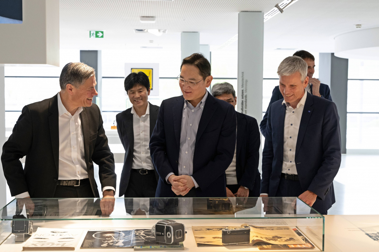
Samsung Electronics Chairman Lee Jae-yong met with top executives of German optics manufacturer Zeiss, a crucial partner for the Korean tech giant's push to lead the burgeoning market for artificial intelligence chips, during his recent trip to Europe.
According to Samsung on Sunday, its chief toured the Zeiss headquarters in Oberkochen on Friday and discussed long-term partnerships with Zeiss Group CEO Karl Lamprecht and Zeiss Semiconductor Manufacturing Technology CEO Andreas Pecher.
Lee's trip to Europe comes at a time when Samsung, the world's top memory chip maker, is expanding its foundry and logic chip businesses with demand for advanced chips on the rise. According to the tech giant, Lee will also travel to France and Italy to meet with business counterparts and inspect the company's European operations.
Zeiss is an optical system manufacturer that has unique technologies for lithography optics and photomask systems used in advanced chip manufacturing equipment.
Zeiss has more than 2,000 patents for key technologies related to the extreme ultraviolet lithography process, a critical technology in producing highly advanced chips. According to Samsung, Zeiss supplies more than 30,000 parts for one extreme ultraviolet lithography machine produced exclusively by ASML, which is based in the Netherlands.
During Lee's visit, Zeiss reaffirmed its commitment to investing 4.8 billion won ($3.4 million) in Korea to build a research and development center by 2026.
Samsung said the collaboration with Zeiss would help the company improve the performance of its next-generation chips, better optimize the manufacturing process and achieve a higher yield rate.
Samsung plans to adopt the advanced EUV technology in its chip manufacturing this year for the production of sixth-generation 10 nanometer DRAM. The company also said it will use the EUV technology to lead the under-3 nm process to make highly advanced semiconductors.
Chip giants are fiercely competing to get ahead in the advanced chip market.
TSMC, the world's top contract chip manufacturer with over 60 percent share of the foundry market, recently announced it will introduce the 1.6 nm process and start producing chips based on cutting-edge technology from the second half of 2026.
Intel also said it will start mass production with the 1.8 nm process from the end of this year, while Samsung Electronics said it will start mass production of chips with the 2 nm process in 2025.
By 2027, all three chipmakers aim to adopt the 1.4 nm process in chipmaking.
On the visit to the Zeiss headquarters, Lee was accompanied by Song Jai-hyuk, the chief technology officer and president at the Samsung’s division in charge of semiconductor business, and Nam Seok-woo, the president in charge of global manufacturing and infrastructure of the division, Samsung said.
Amid the AI boom, Lee is seen ramping up efforts to strengthen ties with global IT giants for chip collaboration. Lee met with Meta CEO Mark Zuckerberg in February and ASML CEO Peter Wennink in December 2023. He also met with Nvidia CEO Jensen Huang in May 2023 to discuss collaboration on advanced AI chips.