First-generation semiconductor equipment and technology venture
AI chips tackled through 'high-rise building' architecture
3D packaging seen solving speed, heat and power efficiency
Solar energy business also gaining momentum
"Market cap of 400 trillion won ($266 billion) is an achievable goal —
the strategy for being No. 1 is taking the road no one has traveled"
![[Courtesy of Jusung Engineering]](https://wimg.heraldcorp.com/news/cms/2026/06/01/news-p.v1.20260429.2b59603286a3440fa3102de0dc8de31e_P1.png)
"What you truly have to stake your life on is the 1 percent of innovation that no one else has imagined or attempted. That is Jusung Engineering's permanent direction."
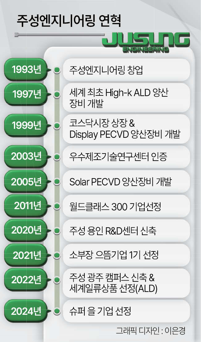
Hwang Cheol-ju, chairman of Jusung Engineering and a pioneer of South Korea's first-generation venture industry, founded the company in 1993 with a dream he called "technological independence for Korea." Witnessing a country that could not manufacture even the screws inside semiconductor equipment, Hwang threw himself into entrepreneurship driven by a single conviction: the need for homegrown technology.
Thirty years on, Jusung Engineering has established itself as a front-end process equipment maker for semiconductors, displays and solar cells. The company not only succeeded in localizing key semiconductor front-end equipment but has taken South Korean machinery global, with atomic layer deposition, or ALD, equipment as its flagship product.
Hwang's philosophy is visible even in how employees address one another. Rather than conventional titles such as assistant manager or department head, Jusung staff use "PL" — short for "Player" — reflecting the idea that every individual is a "national team representative" of technology.
Throughout the company, walls carry aphorisms that distill Hwang's worldview: "Innovation, being No. 1, and success are the results of doing better first"; "Technology equals knowledge plus the five senses; innovation equals technology plus inspiration"; and "Jusung is where happiness is made; home is where happiness is enjoyed." Creating sustainable "happiness" by combining innovation with customer trust is, in Hwang's telling, the company's ultimate purpose.
![Jusung Engineering Chairman Hwang Cheol-ju stressed the need for "innovation without competitors" when speaking to younger small and medium-sized enterprise entrepreneurs in an interview. [Courtesy of Jusung Engineering]](https://wimg.heraldcorp.com/news/cms/2026/06/01/news-p.v1.20260429.8b109062ed344935982b04397d91f2c6_P1.png)
Logic and memory in one space: AI chips reimagined as 'high-rise buildings'
Jusung Engineering's signature technology is the ALD mass-production equipment it developed in 1997 — the world's first of its kind. Deposition refers to the process of forming a thin film on a semiconductor surface. As semiconductor patterns have shrunk to the nanometer scale, ALD has become a core technology in front-end semiconductor manufacturing. Hwang also serves as chairman of SK Hynix's cooperative growth council.
"The growth of AI resembles the growth of a human being — learning language, learning logic, then moving on to reasoning," Hwang said. "In that process, memory chips play the role of a library. Demand will surge at least a hundredfold from current levels, and semiconductors will improve in ways we cannot yet predict."
He identified the distance between logic chips, which handle computation, and memory chips, which store data, as the source of a critical bottleneck. Most AI chips today rely on 2.5D packaging, which places logic and memory side by side on a horizontal plane.
"Transistors have shrunk to the 1-nanometer level, but the problem is fetching data from memory sitting about 1 centimeter away," Hwang said. "It is like data making hundreds of round trips between Incheon and San Francisco — it creates a massive data bottleneck and consumes enormous amounts of power."
Simply shrinking logic chips further to 1 nanometer, or boosting memory performance alone, amounts to incremental improvement rather than a solution to the underlying problem, he said. Hwang's answer is vertical stacking — 3D packaging: stacking memory on top of logic and logic on top of memory, creating a single "high-rise building" where everything operates in one space at the same speed, much like the human brain.
"Since the transistor was invented in 1947, semiconductor architecture has essentially been about cramming more detached houses — circuits — onto a fixed plot of land," Hwang said. "Data moves horizontally, consuming a lot of power and generating heat. But if you build chips like a high-rise apartment, where people move quickly by elevator, you can solve all three problems at once: speed, heat and power efficiency."
Shifting the paradigm to semiconductor production without silicon
Building chips like high-rise buildings requires a special class of semiconductor material, Hwang said — and Jusung Engineering has developed what it calls the world's first atomic layer growth, or ALG, equipment. Conventional ALD could only produce Group III-V semiconductors at temperatures above 1,000 degrees Celsius and on sapphire substrates, but ALG technology enables mass production on any substrate at temperatures below 400 degrees Celsius.
ALG makes it possible to manufacture semiconductors without silicon, the material that has long been the industry's foundation. SK Group Chairman Chey Tae-won has said that memory supply shortages stem from wafer shortages — and ALG technology could, in principle, overcome physical supply constraints through engineering alone. Beyond reshaping the semiconductor process paradigm, the technology offers compelling economics: unlike round silicon wafers, glass substrates are rectangular, making them more than 30 percent more efficient in material use and more than 10 times cheaper.
"If conventional deposition equipment works like snow accumulating layer by layer, ALG works like water freezing into ice," Hwang said. "Just as ice can take many forms — thin ice, solid ice — semiconductors can be built in 3D shapes. Applying this equipment should allow us to overcome many of the industry's longstanding challenges."
The market is beginning to take notice. According to industry sources, Jusung Engineering recently supplied semiconductor equipment capable of implementing ALG technology to a prominent overseas manufacturer.
Explosive growth on the scale of Nvidia and Tesla
Jusung Engineering is focused on creating new markets with products it describes as "world firsts and one-of-a-kind."
"Innovation has no competitors. What has competitors is technology," Hwang said. "No matter how good a technology is, if competitors exist in the market, the buyer sets the price — not the maker. But with innovation, even if it is imperfect, there are no competitors, so the maker sets the price. That is how you generate profit." He described this as the core of his management philosophy.
Jusung's technology also underpins South Korea's rise to global dominance in DRAM. Memory chips are built from combinations of transistors and capacitors. Jusung developed the world's first selective HSG deposition equipment dedicated to capacitors in 1995, and in 1997 became the first company in the world to bring ALD equipment to mass production.
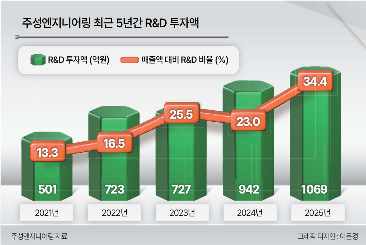
"The only way for someone born with nothing to end up with everything is technology," Hwang said — explaining why the company consistently reinvests 20 to 30 percent of sales into research and development. As of 2024, roughly 63 percent of Jusung's total workforce is engaged in R&D, and the company holds a cumulative patent portfolio of more than 3,220 patents. After building a new R&D center in Yongin in 2020 and a campus in Gongju in 2022, the company plans to invest approximately 104.8 billion won to establish a second research institute in Yongin by 2028.
Beyond semiconductors, which currently account for more than 70 percent of sales, Jusung plans to lead new markets in solar energy. The company believes solar will eventually supply 30 percent of the world's energy and is accelerating development of solar power generation technology.
Jusung is developing what it calls "tandem solar cell" technology by combining the CVD, ALD and ALG deposition techniques it has refined in semiconductors. The company sees this technology eventually expanding into displays and serving as a power source for space-based AI data centers.
"Jusung is the only company that holds all three core processes — CVD, ALD and ALG," Hwang said. "The energy market is far larger than semiconductors, and solar is at the heart of it. Jusung is developing solar power generation technology that can replace nuclear power plants, batteries and hydrogen."
Industry insiders say Jusung Engineering could be positioned to enter the solar equipment supply chains of global big-tech companies. Hwang also raised the prospect of reaching a market capitalization of 400 trillion won ($266 billion), grounding the ambition in competitive benchmarks. "The companies called our rivals are Applied Materials and Lam Research in the United States, and Tokyo Electron in Japan," he said. "Each of them has surpassed a market cap of 400 trillion won, and Tokyo Electron has exceeded 200 trillion won." He said reaching 200 trillion won is a fully attainable goal, and signaled that doubling that figure to 400 trillion won is also within reach.
Hwang drew a distinction between innovative companies and imitators, citing Nvidia and Tesla as examples. When Nvidia listed in 1999, its market capitalization stood at roughly 300 billion won. Twenty-seven years later, after a long incubation period, it has grown to 7,000 trillion won — an increase of more than 23,000 times. Hwang said he is confident Jusung can follow a similar trajectory.
Imitation cannot generate profit — innovation is urgent for small and medium-sized enterprises
True to his reputation as the "godfather of K-materials, parts and equipment," Hwang offered pointed criticism of the domestic corporate ecosystem. While large companies such as Samsung Electronics and SK Hynix have seen their share prices soar, the number of companies delisted from the Kospi and Kosdaq in the first quarter reached a record high of 15 — a sign, he said, of a deepening K-shaped polarization in growth.
Hwang said South Korea's economy can only generate additional value by moving beyond an imitation-based model toward an innovation-driven one. "Until now, this country has stopped at copying others' technology faster and cheaper under the banner of localization," he said. "Selling cheaply through imitation can no longer generate meaningful profit. To make a profit, you need innovation — something with no competitors."
He said the urgency of innovation is even greater for small and medium-sized enterprises. "Cooperation means sharing your own capabilities, but sharing your capabilities keeps you in a vertical, subordinate relationship where profit is impossible — that is the typical structure of the Korean corporate ecosystem," Hwang said. "What is needed is collaboration: sharing the results of what you do well, without giving away your competitive edge. That enables horizontal partnerships and opens the path to an innovation economy."
He went on to say, "The goal of being No. 1 and the goal of being No. 2 are different. No. 2 only has to chase. There is no need to take on risk. But No. 1 has no one to chase — you have to overcome risk on your own. South Korea has now entered the moment when it must be No. 1. That means taking the road no one has traveled."
Standing at a crossroads between being overtaken and remaining the world's first and best, Hwang also stressed the role of government.
"A country driven by fixed ideas and entrenched interests cannot become an advanced nation," he said. "Innovation must be nurtured, not managed. If you close off the market, innovation dies."
go@heraldcorp.com