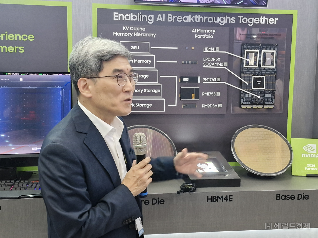
DS division CTO Song Jae-hyeok holds tech briefing
Less than three months after HBM4E sample debut in the US
Next-generation heat management technology HPB applied
Samsung signals firm intent to lead next-gen HBM market
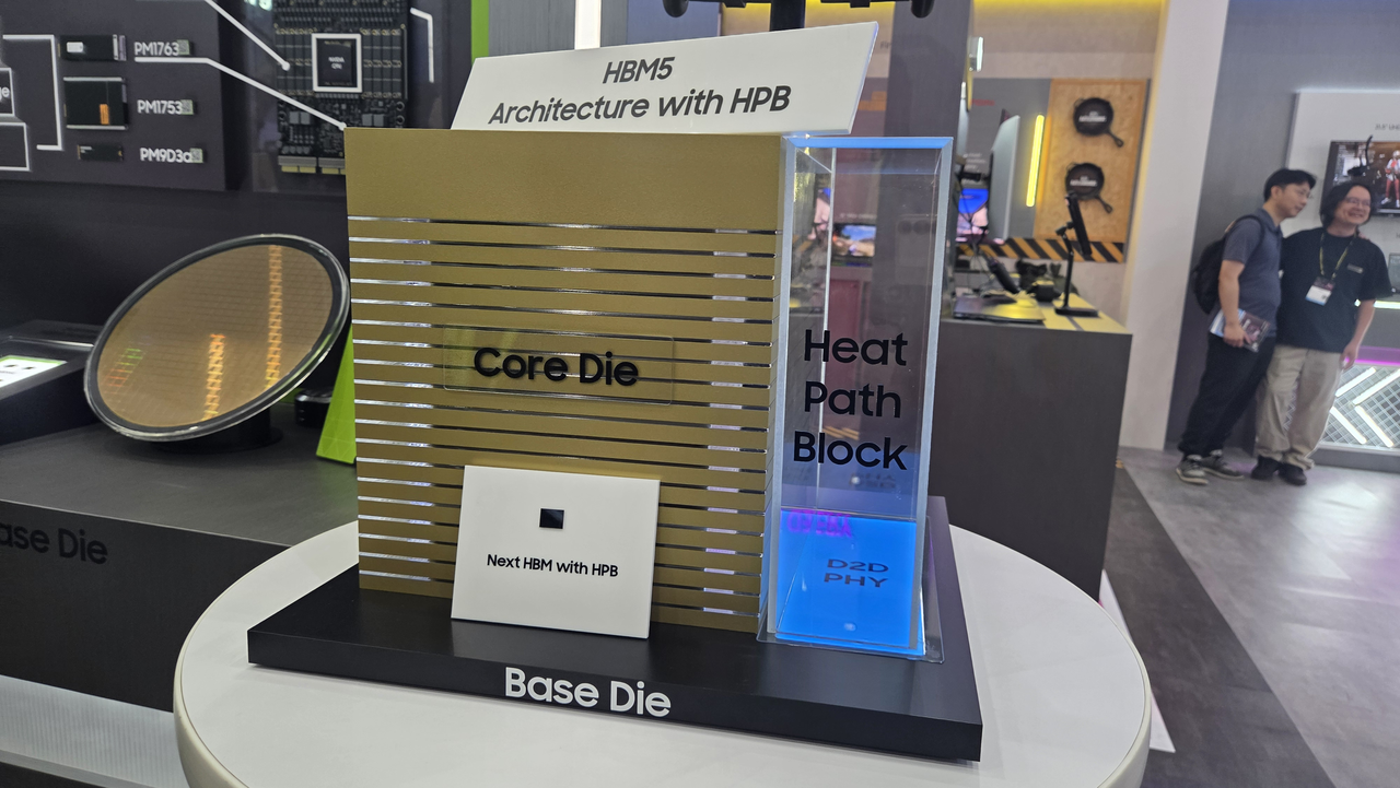
Samsung Electronics unveiled the industry's first physical mock-up of HBM5, its eighth-generation high-bandwidth memory chip, at Computex 2026, Asia's largest IT trade show, signaling its intent to lead the next-generation HBM market. The reveal came less than three months after the company showed an HBM4E sample — its seventh-generation HBM.
Speaking at a technology briefing Monday morning local time, Samsung's semiconductor (DS) division Chief Technology Officer Song Jae-hyeok said the company could not disclose exact launch timelines for HBM4E and HBM5, but added that it could adjust its schedule flexibly based on customer needs and end-market demand.
Samsung had previously unveiled an HBM4E sample at Nvidia GTC 2026 in San Jose in March. The HBM5 mock-up at Computex marks the company's second major HBM reveal in under three months.
HBM sits alongside a GPU, but a bottleneck known as the "memory wall" arises when memory data transfer speeds cannot keep pace with the processing speeds of CPUs or GPUs.
Addressing that bottleneck requires higher bandwidth, which in turn generates intense heat — a persistent industry challenge. To tackle this, Samsung applied a next-generation heat management technology called HPB to HBM5, designed to efficiently distribute and dissipate heat produced in the PHY (Physical Layer) area beside the core die.
By integrating the technology into an actual product, Samsung said it has completed comprehensive verification covering not only structural design but also reliability and package stability.
SK Hynix is pursuing a similar approach with its iHBM technology, which embeds Integrated Cooling Elements (ICE) directly into the HBM package to dramatically reduce heat generation.
Song described HBM as "a domain of total artistry," adding that Samsung is "the world's only IDM (integrated device manufacturer) capable of supplying integrated technology spanning memory, foundry and packaging."
The HBM5 core die is expected to use 1c (10nm-class sixth-generation) DRAM. Song said the 1c DRAM, Samsung's most advanced process node, "is showing increasingly mature performance, yield and quality over time."
The HBM5 base die is expected to adopt a 2-nanometer advanced process. Song said the move would allow Samsung to "provide an optimized solution that simultaneously meets the bandwidth and power requirements the market demands."
Samsung also displayed HBM4E wafers and chipsets at the event. HBM4E combines a cutting-edge 1c DRAM core die with a 4-nanometer base die from Samsung's own foundry. Samsung completed the industry's first HBM4E sample shipment on May 29, with the chip operating stably at 14 gigabits per second per pin and capable of reaching up to 16 Gbps — equivalent to a maximum of 4 terabytes per second — a result seen as validating the company's advanced process capabilities.
Song said Samsung is developing technology "with a sense of urgency," pledging to "prepare and strive to be No. 1 in technology." He added that the company plans to keep strengthening its next-generation memory technology competitiveness "through collaboration with global companies, including Nvidia."
Nvidia CEO Jensen Huang said the company continues to receive strong support from its global semiconductor supply chain partners, but that supply of Nvidia chips "remains constrained."

go@heraldcorp.com