Industry-leading data transfer bandwidth based on V9 NAND
Power efficiency improved 40% over UFS 4.1
Package 16.7% smaller than predecessor, with up to 1TB capacity
Mass production from Q4 this year; to be used in next-generation premium mobile, wearable and XR devices
Move aimed at strengthening grip on global NAND market
![Samsung Electronics' UFS 5.0 product [Samsung Electronics]](https://wimg.heraldcorp.com/news/cms/2026/06/23/news-p.v1.20260623.7704b202285d447bbd84c2eed95d0d4c_P1.jpg)
Samsung Electronics said Tuesday it has developed the industry's first next-generation Universal Flash Storage (UFS) 5.0 memory solution optimized for the on-device AI era, claiming the highest performance in the industry.
UFS is a high-performance storage standard used in mobile devices such as smartphones and tablets, prized for its fast data transfer speeds and high power efficiency. On-device AI refers to running AI models directly on a device without a network connection.
The new product adopts the UFS 5.0 interface, the latest embedded memory standard from semiconductor standards body JEDEC. Built on Samsung's advanced ninth-generation V-NAND (V9), it achieves both an industry-leading data transfer bandwidth of 10.8 gigabytes per second and high power efficiency.
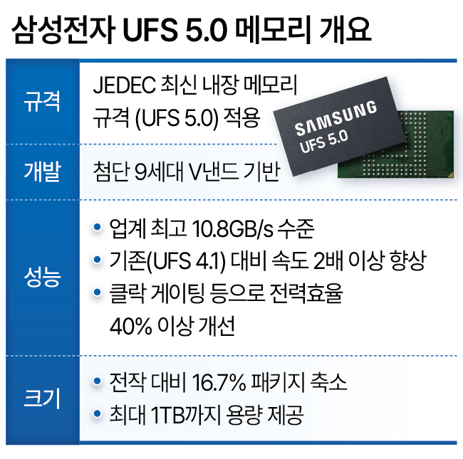
As generative AI shifts from cloud-centric to on-device processing, the volume of data that mobile devices must handle internally has grown sharply. Storage is evolving beyond simple data retention into a core piece of infrastructure that underpins AI computation.
Samsung's UFS 5.0 supports sequential read speeds of 10.8 GB/s and sequential write speeds of 9.5 GB/s — more than double the performance of the previous UFS 4.1 — enabling faster storage and processing of large volumes of data.
The product is optimized for the diverse data-processing demands of AI applications, reducing latency in on-device AI environments and supporting faster AI service response times.
UFS 5.0 also improves power efficiency by more than 40 percent over its predecessor through several new technologies tailored for next-generation mobile low-power environments: clock gating, which boosts power efficiency by cutting the operating signal to circuits not in use, and multi-voltage, which reduces power consumption and heat by applying the optimal voltage to each circuit.
As a result, the product significantly lowers the power consumed when transferring the same amount of data, extending battery life in mobile devices.
Samsung has designed the UFS 5.0 in a package measuring 7.5 mm wide, 13 mm long and 0.9 mm tall — 16.7 percent smaller than its predecessor — to improve design flexibility and space efficiency in mobile, wearable and XR (extended reality) devices, while offering capacity of up to 1 terabyte.
As on-device AI use expands, mobile storage is becoming an increasingly critical factor in determining the performance and user experience of mobile devices.
Samsung plans to begin mass production of UFS 5.0 in the fourth quarter of this year to get ahead of market demand, and intends to expand supply in step with the growth of next-generation device markets — including not only flagship smartphones but also XR headsets and AI wearables.
The company aims to further cement its leadership in the global NAND market through the development and mass production of UFS 5.0. According to market research firm TrendForce, Samsung held a 31.6 percent share of the NAND market by sales in the first quarter of this year, up 3.6 percentage points from the previous quarter, widening its lead over second-place SK Hynix, which held 17.6 percent including Solidigm.
"In the on-device AI era, storage is becoming more than just a place to keep data — it is a defining element of the AI experience," said Choi Jang-seok, senior vice president and head of product planning at Samsung Electronics' Memory Business. "By completing the industry's first UFS 5.0 development, Samsung Electronics is setting a new standard for next-generation mobile storage and will continue to lead innovation in AI mobile."
gil@heraldcorp.com