- SiC defect emission wavelength confirmed at 459 nm, not 424 nm
- Findings lay groundwork for revising international SiC semiconductor standard
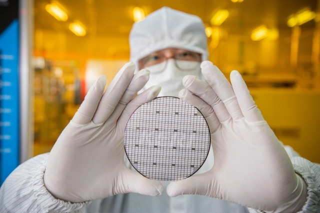
A team of South Korean researchers has uncovered a 15-year-old error embedded in the international standard used to detect defects in next-generation power semiconductors found in electric vehicles and renewable energy systems. Using atomic-level analysis, the team demonstrated that the light wavelength used to identify a specific internal defect differs from the value long accepted by the industry. The findings are expected to improve the accuracy of power semiconductor quality inspections and help reduce defect rates in manufacturing.
The Korea Electrotechnology Research Institute (KERI) announced Sunday that a research team led by Dr. Na Mun-gyeong of its Next-Generation Semiconductor Research Center, working jointly with Chungnam National University, Horiba Stec Korea and SK Siltron, had confirmed that the emission wavelength used to identify defects in silicon carbide (SiC) power semiconductors is 459 nanometers (nm) — not the 424 nm figure that had been in use.
SiC power semiconductors are key components widely used in electric vehicles and solar and wind power installations because they operate reliably under high voltage and temperature conditions.
During manufacturing, however, a phenomenon called "stacking faults" — in which atomic layers deviate from their normal arrangement — can degrade the performance and reliability of a power semiconductor. Detecting these faults accurately is central to semiconductor quality control.
The industry uses a technique called photoluminescence (PL) inspection, which shines light on a semiconductor wafer and measures the wavelength of the light emitted in return, without damaging the wafer. Each type of defect emits light at a characteristic wavelength, effectively serving as a fingerprint.
The problem is that the wavelength data used for roughly 15 years to identify one particular defect type has been wrong.
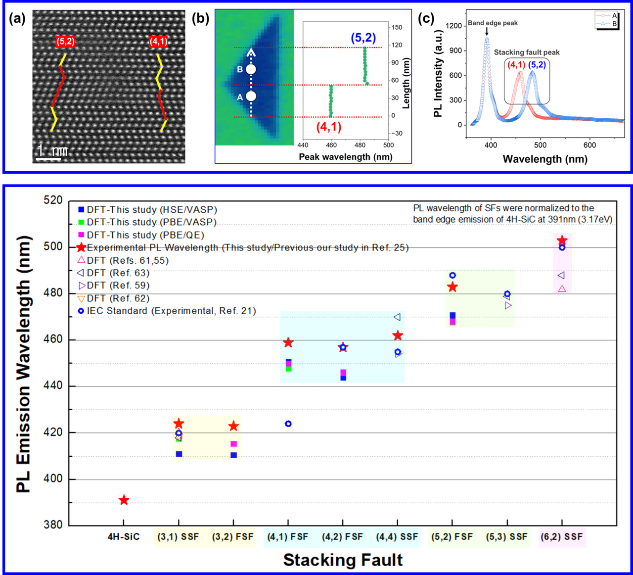
The International Electrotechnical Commission (IEC) standard had recorded the "(4,1) Frank-type stacking fault" as emitting light at 424 nm. But direct verification of whether that wavelength accurately corresponded to the actual atomic arrangement had been lacking.
The research team analyzed more than 100,000 defect data points collected from 207 commercial SiC wafers to track the characteristics of Frank-type stacking faults.
After locating defects using light, the team precisely cut out the relevant sections at the nanometer scale and examined the actual atomic arrangement using an atomic-resolution scanning transmission electron microscope.
A total of 176 ultra-thin specimens were prepared for this purpose, and the results were cross-verified through theoretical calculations performed on a supercomputer.
The team confirmed that the true emission wavelength of the "(4,1) Frank-type stacking fault" — previously recorded as 424 nm — is in fact 459 nm.
The research is significant in that it provides a scientific basis for correcting an error in a defect identification standard that has been in use for a long time.
By directly linking a defect's light signal to its actual atomic structure, researchers can now more accurately trace the causes of defects that arise during semiconductor manufacturing. The findings are also expected to contribute to improvements in manufacturing processes and to higher yields and reliability in power semiconductors.
The research was published in Acta Materialia, an international journal in the field of materials science.
Na was recognized for this research and other work on SiC semiconductor defect analysis, receiving an Honorable Mention at the 2026 Horiba Masao Award, an international research prize. It marks the first time a researcher affiliated with a domestic research institution has received the honor since the award was established in 2004.
"It is deeply meaningful to have corrected a long-entrenched error in a global identification standard by directly linking light signals to actual atomic structures," Na said. "We will continue to build the foundation for strengthening the quality competitiveness of South Korea's power semiconductor industry."
nbgkoo@heraldcorp.com