- Threaded grooves on lens suppress noise
- Pinpoint detection of micro-defects without damaging chips
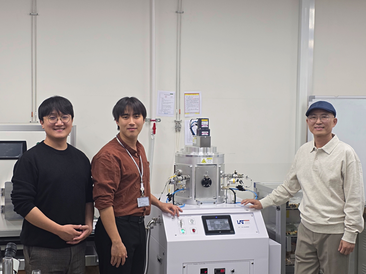
South Korean researchers have developed an ultrasonic sensor capable of clearly detecting microscopic cracks and air voids inside semiconductor chips without cutting or damaging them. The key innovation is a series of threaded grooves carved into the side of the lens to suppress the noise that degrades image clarity.
Daegu Gyeongbuk Institute of Science and Technology (DGIST) announced Wednesday that a research team led by Professor Jang Jin-ho of the Department of Electrical Engineering and Computer Science had developed a "threaded-lens focused ultrasonic sensor" capable of precisely identifying ultra-fine defects inside semiconductors.
In the electric vehicle and aerospace industries, the reliability of power semiconductors — which must withstand high voltages and heat — is critical. Microscopic cracks or voids inside a semiconductor can lead to degraded performance and device failure.
Non-destructive ultrasonic testing is used to detect such defects, but conventional sensors have struggled to image fine internal structures clearly because ultrasonic waves bouncing repeatedly inside the lens generate noise that obscures detail.
The problem is compounded in industrial inspection equipment, where tight installation spaces make it difficult to simply increase sensor size.
The research team drew inspiration from the wedge-shaped sound-absorbing structures found in anechoic chambers, which are designed to minimize acoustic reflections. They carved densely spaced, angled threaded grooves into the side of the ultrasonic lens so that reflected waves scatter in multiple directions rather than converging.
The design suppresses the noise caused by reflected waves concentrating at a single point inside the lens, while leaving the sensor's overall size and core components unchanged.
Through computer simulations, the team confirmed that a thread height of 500 micrometers and an inclination angle of 30 degrees represent the optimal design conditions, balancing noise suppression with ease of fabrication.
When applied to a power semiconductor module for automotive use, the sensor successfully imaged internal structures — including metal wires roughly one-quarter the width of a human hair and tiny air bubbles — that had been obscured by noise in conventional sensors. The team said the resulting image clarity is comparable to that of computed tomography.
The technology has a practical advantage: it requires only the addition of side-surface machining to the lens, while retaining existing piezoelectric components and assembly processes, making it relatively straightforward to deploy in industrial settings.
The team expects the sensor to find applications in inspecting power semiconductors for electric vehicles and aerospace systems, as well as detecting voids, delamination and micro-cracks inside multilayer semiconductor packages. It could also be extended to high-resolution acoustic microscopy and medical ultrasonic sensors.
However, the threaded structure will need to be re-optimized depending on the ultrasonic frequency and lens material used, and integration with automated high-speed inspection equipment will require further validation. The team estimates commercialization is about two years away.
"The significance of this work lies in solving what has long been the biggest challenge for industrial ultrasonic sensors — internal lens noise — through a simple geometric modification," Jang said. "Going forward, we will expand verification of real-world process defects through joint research with semiconductor manufacturers and accelerate the development of next-generation non-destructive inspection systems."
DGIST postdoctoral researcher Kang Seong-hu and integrated master's-doctoral student Park Hyeon-gyu served as co-first authors on the study. The findings were published in NDT & E International, a peer-reviewed journal in the field of non-destructive testing.
nbgkoo@heraldcorp.com