- Used equipment transferred to Korea Nanotechnology Institute
- Idle equipment to support materials, parts and equipment technology development
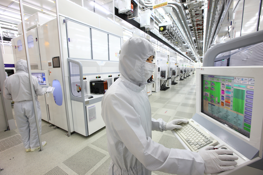
Samsung Electronics will share factory operation know-how and equipment accumulated at its world-class semiconductor manufacturing facilities with domestic public research institutions.
South Korea's Ministry of Science and ICT said Wednesday it would hold a consulting results presentation and used-equipment transfer ceremony at the Korea Nanotechnology Institute in Suwon, Gyeonggi Province, marking the outcome of a collaboration between Samsung Electronics and the institute on improving the efficiency of public nanofab operations.
The initiative follows up on a memorandum of understanding the ministry signed in March last year with three major domestic semiconductor companies — Samsung Electronics, SK hynix and DB HiTek.
Samsung Electronics' DS Division Co-Prosperity Center conducted semiconductor fab operation and management consulting for the Korea Nanotechnology Institute from June through October. The effort extended private-sector manufacturing innovation know-how — previously applied to the National NanoFab Center and the Nano Convergence Technology Institute — to a public research institution.
In particular, Samsung Electronics adapted its "materials, parts and equipment eye-level consulting" program, originally developed for supply-chain partners in those sectors, to suit the characteristics of public nanofab operations.
Standard operating procedures, inspection checklists, and training and operational guidelines were updated for each piece of equipment. A field inspection manual drawn from Samsung's commercial mass-production facilities was developed and applied to a public nanofab for the first time.
The effort laid the groundwork for public nanofabs to carry out safety management and equipment inspections at a level comparable to commercial semiconductor production sites.
Idle semiconductor equipment from Samsung Electronics will also be deployed at public research facilities.
Through the Ministry of Science and ICT's MoaFab used-equipment support project, an automated thin-film pattern measurement system owned by Samsung Electronics will be transferred to the Korea Nanotechnology Institute.
The equipment can precisely measure the thickness and optical constants of single- and multi-layer thin films formed on 8-inch semiconductor wafers without causing damage. The Korea Nanotechnology Institute plans to use it to build an 8-inch automated thin-film measurement capability it previously lacked, and to support technology development for companies, universities and research institutions.
The government plans to extend the collaboration model to other public nanofabs.
The consulting outcomes and field inspection manual will be shared with and sequentially applied to the Electronics and Telecommunications Research Institute's Specialized Semiconductor Technology Center, Seoul National University's Semiconductor Research Consortium and the Daegu Gyeongbuk Institute of Science and Technology's Next-Generation Sensor and Semiconductor Research Institute.
Executive Vice President Ji Hyun-gi, head of Samsung Electronics' DS Division Co-Prosperity Center, said the company would "contribute to a virtuous cycle of mutual growth in which Samsung's accumulated manufacturing innovation know-how flows through public nanofabs and back to researchers and materials, parts and equipment companies."
First Vice Minister of Science and ICT Koo Hyeok-chae said "global semiconductor competition is shifting into a contest that mobilizes the full capabilities of each nation," adding that the ministry would "actively support semiconductor technology innovation and the development of specialized talent by expanding private-sector consulting and idle-equipment transfers to all institutions participating in MoaFab."
nbgkoo@heraldcorp.com