Nanoscale current channels observed in three dimensions; electrode protrusions found to guide filament formation
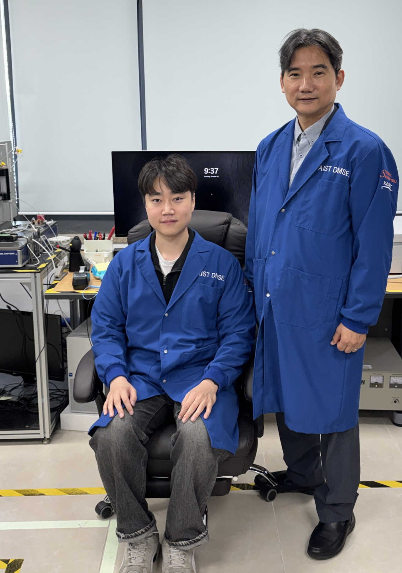
South Korean researchers have mapped the ultrafine pathways through which electricity flows inside next-generation memory chips.
KAIST announced Thursday that a joint research team led by professors Hong Seung-bum and Park Sang-hee of the Department of Materials Science and Engineering had observed the internal current channels of resistive random-access memory (RRAM) in three dimensions and identified how microscopic structures on the electrode surface influence where those channels form.
RRAM is a next-generation semiconductor that stores information by creating or severing conductive pathways. The presence or absence of current flow corresponds to the digital values "1" and "0."
A persistent challenge, however, has been that the location and shape of these current channels vary each time they form, causing inconsistencies in operating voltage and overall performance.
To address this problem, the research team observed in three dimensions the ultrafine current channels — known as conductive filaments — that form inside the memory device.
The team used a conductive atomic force microscope (C-AFM) for the observations. After forming a current channel in a 10-nanometer-thick titanium dioxide layer, the researchers shaved away approximately 0.1 nanometers at a time over 100 passes to analyze the internal structure.
The current channels proved to be funnel-shaped — wider at the top and narrowing toward the bottom electrode. The tips of the channels in particular tended to connect with tiny protrusions on the surface of the lower platinum electrode.
This pattern appeared consistently across five separate current channels formed at different locations.
The research team concluded that electric fields concentrate around the small protrusions on the electrode surface, influencing the direction in which the current channels grow.
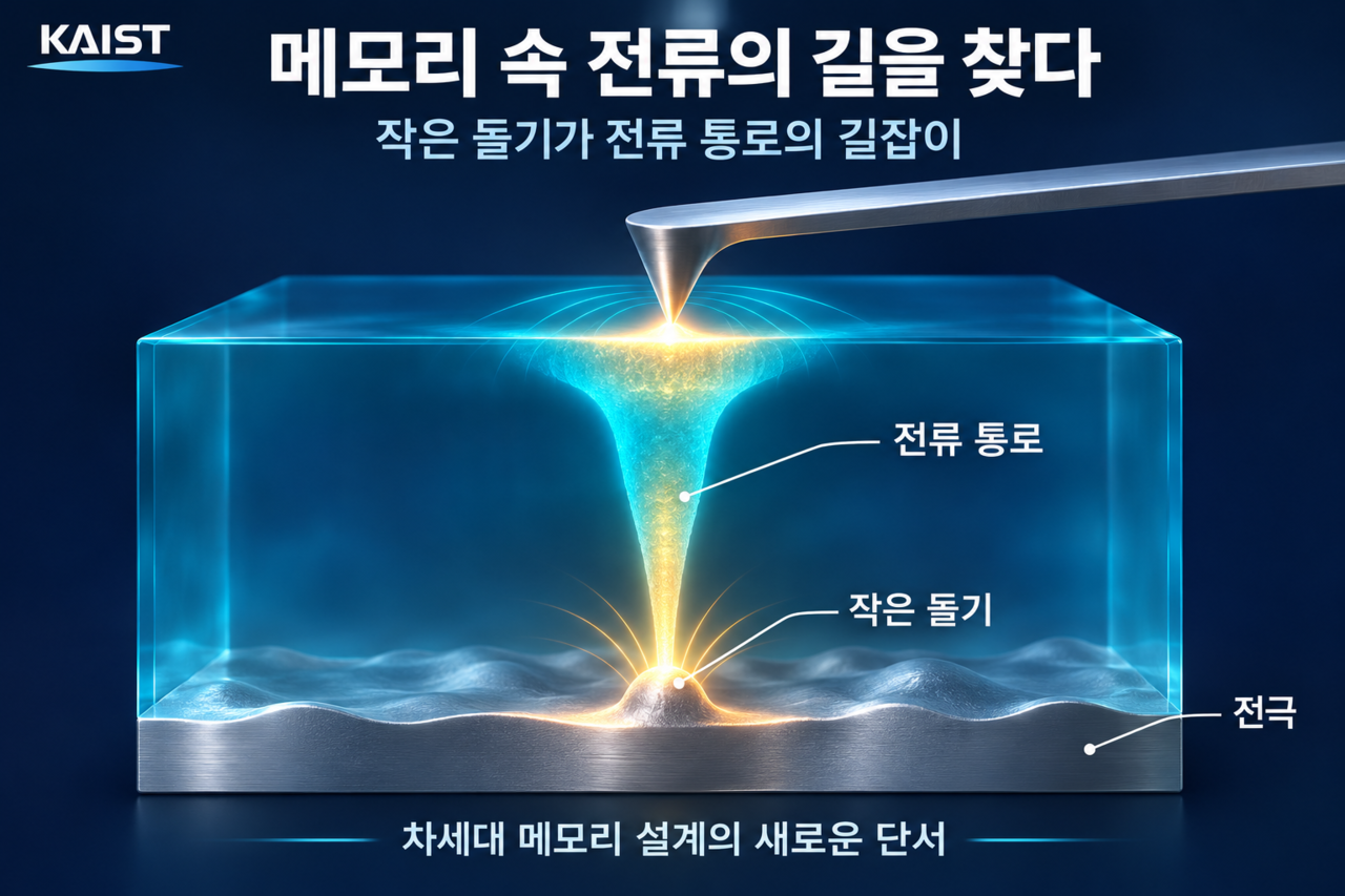
Computer simulations confirmed that electric fields concentrate around the electrode protrusions, supporting the conclusion that the microscopic surface structure of the electrode acts as a guide for current channel formation.
The research team also analyzed the distribution of oxygen vacancies — sites within the current channel where oxygen atoms are missing — which play a key role in filament formation.
The analysis indicated that oxygen vacancies become more concentrated at the center of the channel closer to the lower electrode. The team also suggested that the narrowing of the upper portion of the channel may result from a combination of oxygen vacancy generation and migration.
The significance of the research lies not only in capturing the three-dimensional shape of the current channels, but in linking where those channels form to the actual nanoscale structure of the electrode surface.
"This research goes beyond simply observing the three-dimensional shape of conductive filaments — it connects their form and tip position to the actual nanostructure of the electrode," Professor Hong said. "If electrode surface structure is incorporated as a design variable, it could provide an important foundation for developing next-generation RRAM devices that operate more reliably."
The findings were published online in the international journal Nano Letters on Aug. 11.
nbgkoo@heraldcorp.com