Samsung and SK Hynix bring regional semiconductor investment back into focus as the Jeonnam-Gwangju integrated city prepares to launch, with chipmaking set to spread beyond the Greater Seoul area in line with the government's balanced regional development push
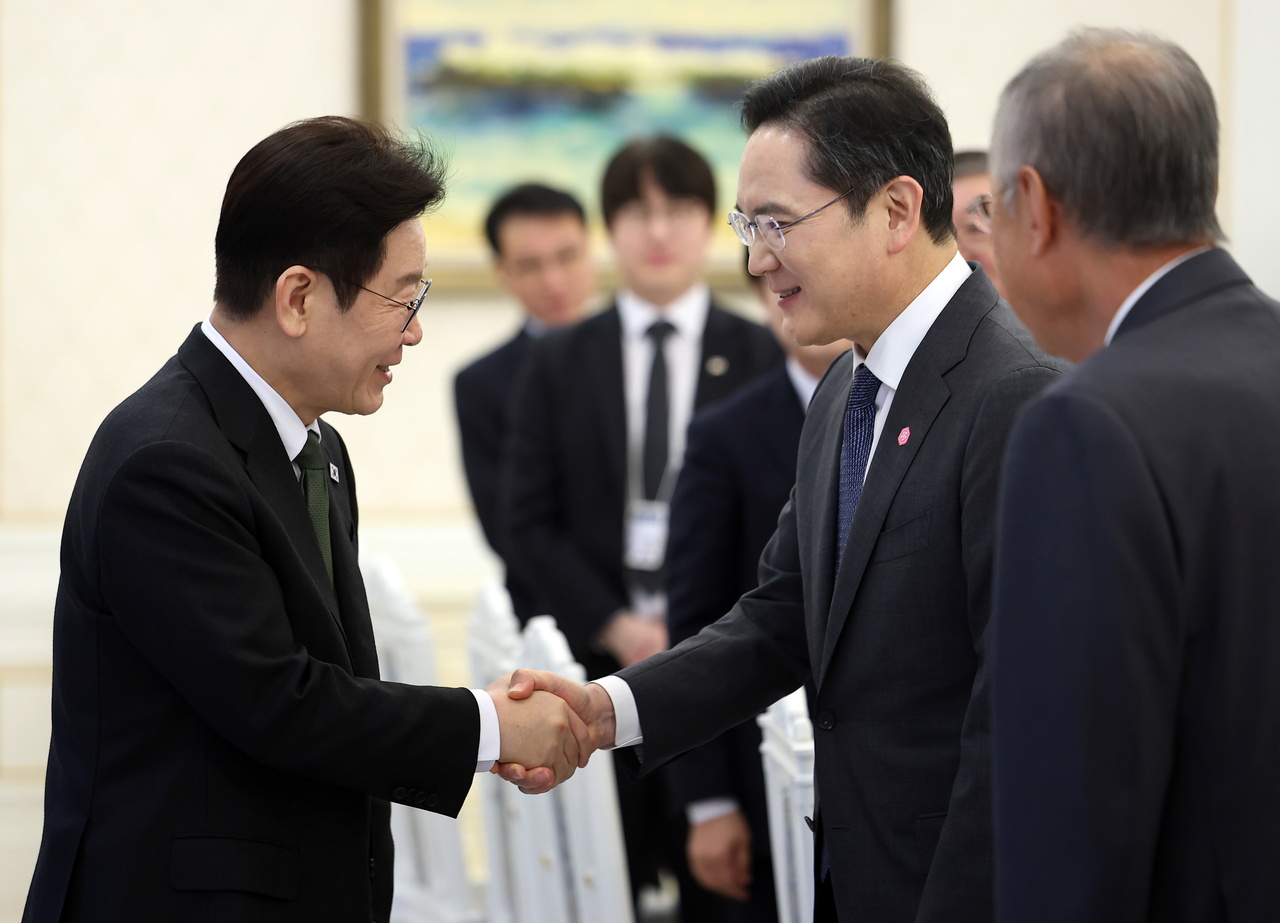
![Plans for new semiconductor production facilities by Samsung Electronics and SK Hynix in the Honam region have resurfaced. Top: Samsung Electronics Chairman Lee Jae-yong meets President Lee Jae Myung at Cheong Wa Dae in February at a business roundtable on youth employment and regional investment expansion. Bottom: Samsung Electronics' Onyang plant in Asan, South Chungcheong Province. [Yonhap/Samsung Electronics]](https://wimg.heraldcorp.com/news/cms/2026/06/10/news-p.v1.20260610.06b5a78feb55485094e9033ff96811d3_P1.jpg)
Plans for new semiconductor production facilities by Samsung Electronics and SK Hynix in the Honam region have resurfaced, ahead of the July 1 launch of the Jeonnam-Gwangju integrated special city.
Government and business circles expect the two companies to unveil detailed investment plans at a meeting between President Lee Jae Myung and top executives — including Samsung Electronics Chairman Lee Jae-yong and SK Group Chairman Chey Tae-won — scheduled at Cheong Wa Dae later this month.
Under the scenario being discussed, the semiconductor clusters both companies are building in Yongin, Gyeonggi Province, would proceed as planned, while select facilities such as packaging plants — back-end operations — would be added in regional locations.
The push to decentralize semiconductor production facilities, which lawmakers and civic groups in the Honam region had championed earlier this year, appears to be gaining momentum and moving toward concrete action.
According to political and business sources Wednesday, President Lee's recent first-anniversary press conference remark that he would "soon unveil a large-scale investment project representing a major shift in growth strategy" has drawn fresh attention to regional investment plans by Samsung Electronics and SK Hynix, the two pillars of South Korea's semiconductor industry.
For Samsung Electronics, the option under discussion is building a new semiconductor packaging plant in Gwangju. Packaging is the final stage of chip production, in which individual chips are bonded side by side or stacked vertically and assembled into finished products — a process known as the back-end.
As front-end processes — etching circuits onto wafers at ever-finer scales — approach their physical limits, advanced packaging that bonds or stacks multiple chips to boost performance is growing in strategic importance.
The race to stack more layers in HBM, which is made by stacking multiple DRAM chips vertically, has intensified — moving from eight layers to 12 and now 16 — making next-generation packaging technology a key competitive battleground.
Samsung Electronics currently operates packaging plants in Onyang and Cheonan, both in South Chungcheong Province. Building a new packaging plant in the Honam region would be the company's first there in 35 years since the Onyang plant opened, and would give the region its first Samsung Electronics semiconductor factory.
Sites under consideration include the future mobility national industrial complex being developed in Gwangju and areas around Jangseong-gun in South Jeolla Province, near the KTX Jangseong station. For Samsung Electronics, the move would align with the Lee administration's emphasis on balanced regional development while expanding production capacity to meet surging demand for AI memory chips.
SK Hynix, meanwhile, broke ground in January on an advanced packaging plant — designated P&T7 — at the Technopolis industrial complex in Cheongju, North Chungcheong Province, with a total investment of 19 trillion won (about $13 billion). The company aims to create synergies by linking front-end and back-end processes at Cheongju, which already serves as its main HBM production base.
Should SK Hynix expand its packaging capacity further, it is expected to diversify its domestic production footprint as part of a contribution to balanced regional development — potentially adding another packaging plant in the Chungcheong region or establishing a new one in the Honam region.
Both companies, however, said "nothing has been decided yet."
The special law on establishing the Jeonnam-Gwangju integrated special city, which passed the National Assembly plenary session in March, allows the minister of the Ministry of Trade, Industry and Energy to designate the area as a semiconductor industry specialized zone on a priority basis if the city's mayor requests it. Under the law, the state must swiftly develop and provide infrastructure — including power, water, waste treatment and roads — for such a zone, with costs covered in full or in part according to standards set by presidential decree.
The push for regional chipmaking gained traction after a December strategy briefing on nurturing the semiconductor industry in the AI era, chaired by President Lee, where power supply for the Yongin semiconductor cluster being developed by Samsung Electronics and SK Hynix was flagged as a major challenge. Calls for new semiconductor plants to be built in regional areas such as the Honam region began to emerge from that point.
When it was pointed out that transmitting power generated from the renewable energy-rich Honam region to Yongin would require running transmission lines through North Jeolla and South Chungcheong provinces — raising local acceptance concerns — President Lee said he hoped that, "from a balanced development standpoint, production would take place in the regions as much as possible."
Lawmakers from Honam constituencies and civic groups subsequently pushed hard for relocating the Yongin semiconductor cluster to the Honam region, causing considerable turbulence in the semiconductor industry.
Political circles and the semiconductor industry then proposed a middle path: proceed with the Yongin cluster as planned, while directing additional investment to regional areas.
Park Gyeong-deok, a semiconductor engineering professor at Pohang University of Science and Technology, said at a K-Semiconductor Triangle forum series in February that concentrating a semiconductor cluster in one location offers advantages in accommodating skilled workers and boosting productivity. He warned, however, that "natural disasters, geopolitical tensions and energy supply constraints can pose significant risks." He added that "the Greater Seoul area cluster in Yongin cannot absorb all the energy and water it needs, making a regional dispersal strategy absolutely necessary," and stressed the need for "a forward-looking strategy that disperses facilities to the regions while maintaining current cluster efficiency."
He also flagged the challenge of securing skilled workers, noting that university graduates' strong preference for jobs in the Greater Seoul area makes attracting talent to regional locations difficult. "Securing public transportation, residential and cultural infrastructure is key," Park said.
joze@heraldcorp.com