Mass production to begin in 2027
First-, second-generation PDKs supplied to customers
Third-generation PDK to launch in November
8-inch SiC competition heats up
Race intensifies in next-generation power semiconductor market
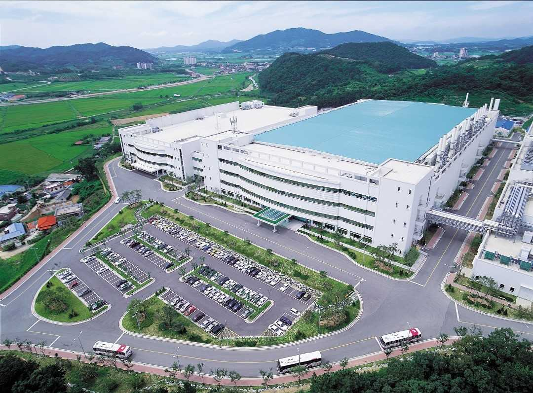
DB HiTek has completed process technology verification for producing silicon carbide (SiC) semiconductors — next-generation power semiconductors used in electric vehicles and renewable energy applications — on 8-inch wafers. The milestone gives the company a foundation to stably produce SiC power semiconductors capable of withstanding voltages of up to 1,200 volts. It plans to begin mass production in 2027.
DB HiTek said Wednesday that it has completed reliability verification of its 8-inch wafer-based 1,200-volt SiC MOSFET (metal-oxide-semiconductor field-effect transistor) process. With this, the company has built the world's first 8-inch SiC foundry process line.
SiC is a next-generation power semiconductor material that outperforms conventional silicon in high-temperature, high-voltage environments. It is used in electric vehicles, renewable energy systems and industrial power equipment, among other applications. While 6-inch wafers remain the mainstream in the SiC market, global manufacturers are accelerating their shift to 8-inch wafers to boost production efficiency and cost competitiveness.
In practice, competition to convert to 8-inch wafers is intensifying worldwide. Infineon began supplying 8-inch SiC-based products last year, and Wolfspeed has since expanded its 1,200-volt SiC MOSFET technology on an 8-inch production platform.
In response, DB HiTek has developed 8-inch SiC process technology optimized for high-power MOSFETs. The company said it has built the world's first 8-inch 1,200-volt SiC foundry process line. This established a foundry service system that supports everything from design to manufacturing, characterization and reliability verification.
DB HiTek is also rolling out process design kits, or PDKs, in stages to support customers' product development. The company is supplying customers with its in-house first- and second-generation 1,200-volt SiC MOSFET PDKs and plans to introduce a third-generation PDK in November. It expects the kits to shorten customers' product development timelines by more than a year.
The second-generation process now available achieves a specific resistance of 2.5 milliohms per square centimeter or less under an 18-volt gate voltage condition. It also achieves a threshold voltage of 3 volts or higher under the same condition. It has also cleared reliability verification, a step with a high technical barrier to entry.
The third-generation process, set to be unveiled in November, aims to lower specific resistance to 2.3 milliohms per square centimeter or less under the same gate voltage condition. DB HiTek also plans to secure a short-circuit withstand time — a measure of how long a power semiconductor can endure a short circuit without damage — of 2.5 microseconds or more.
DB HiTek plans to first offer the process service to customers it has worked with over multiple years, starting in the third quarter of this year. It will then extend the service to all customers from the second quarter of 2027.
"We will thoroughly prepare for 8-inch SiC mass production in 2027 to secure an early lead in the market, and will continue to expand our competitiveness in the next-generation power semiconductor foundry market," a DB HiTek official said.
go@heraldcorp.com