SAFE Forum 2026 held at Seocho headquarters
Process and design innovation strategies presented to attract AI semiconductor customers
High-performance SRAM technology for Nvidia AI chips highlighted
DTCO and next-generation 2nm process technology also showcased
Ecosystem expansion explored with foundry partners
Samsung Foundry Forum dinner to feature President Han Jin-man
Samsung Electronics' foundry division unveiled its next-generation technology roadmap Tuesday at the SAFE (Samsung Advanced Foundry Ecosystem) Forum 2026, laying out its strategy to win over global AI semiconductor customers.
The company highlighted plans to strengthen its SRAM (static random-access memory) technology — which drew attention after being adopted in Nvidia's first AI inference-dedicated chip, the Groq3 language processing unit — and shared its innovation strategy for improving AI semiconductor performance.
The Groq3 LPU is currently in production at Samsung's foundry division. Samsung also displayed the actual Groq3 LPU wafer signed by Nvidia CEO Jensen Huang at GTC 2026 in March, showcasing the close partnership between the two companies.
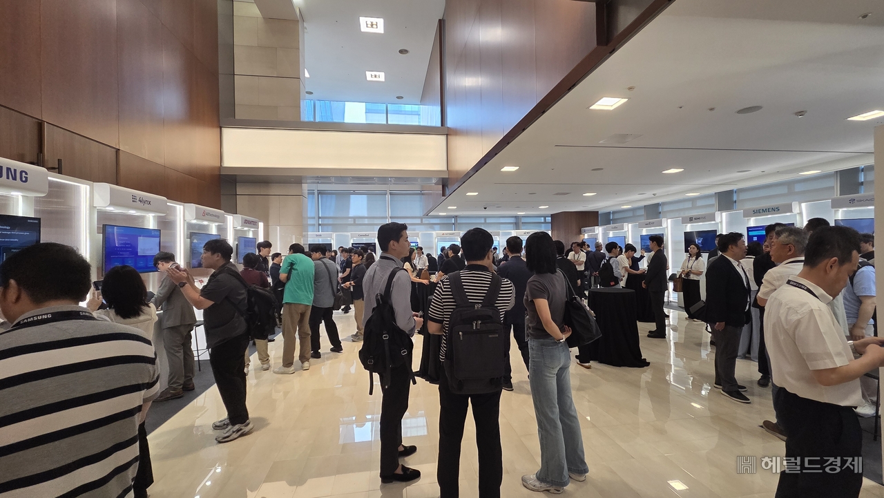
The forum, held at the multipurpose hall of Samsung Electronics' Seocho headquarters in Seocho-gu, Seoul, ran under the theme "The Nexus for Silicon Intelligence." The annual event, where Samsung shares the latest technology trends with its foundry customers and partners, drew about 400 attendees from client and partner companies.
The Samsung Foundry Forum (SFF) 2026, a dinner gathering for C-level executives from customers and partners, is scheduled to follow in the evening. Han Jin-man, president of the foundry division, is expected to attend.
The event drew heightened attention amid growing interest in Samsung Electronics as an alternative to TSMC — the world's top foundry — which has been experiencing supply disruptions due to a surge in AI semiconductor orders.
In the keynote address, Shin Jong-shin, head of Samsung Electronics' foundry design platform development division, said the company is "actively expanding collaboration with global AI and HPC (high-performance computing) customers while also strengthening ties with domestic system semiconductor clients, and will go beyond foundry production to reinforce its role as a platform for the domestic system semiconductor industry."
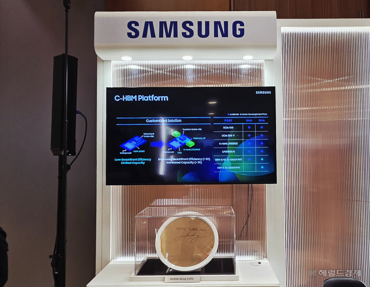
Samsung also presented process and design innovation strategies to boost the competitiveness of its AI semiconductor customers' products. These included DTCO (Design Technology Co-Optimization), which simultaneously optimizes chip design and process technology, as well as next-generation 2-nanometer process technology and process innovation directions tailored for AI semiconductors.
SRAM technology — a key factor in improving AI semiconductor performance — was also in the spotlight. SRAM processes data faster than DRAM, making it highly sought after by big tech companies developing AI chips, though its large cell size and complex circuit structure limit capacity scaling. Samsung said it "continues to improve power, performance and area competitiveness through its DTCO strategy and high-performance SRAM technology, supporting the development of next-generation products demanded by AI semiconductor customers."
Park Sung-hyun, CEO of Rebellions — a domestic AI fabless chip designer that uses Samsung's foundry — took the stage to present on the theme "From Silicon to Mass Production: The Agentic AI Era Opened by Rebellions and Samsung."
Park said the company developed its Rebel100 NPU (neural processing unit) based on Samsung Electronics' 4-nanometer foundry process and advanced packaging, adding that it will "build sovereign AI through collaboration in the AI semiconductor space going forward."
Jean-Marie Brunet, senior vice president at Siemens EDA, which provides electronic design automation software, said "broad support across yield, design verification, reliability and packaging is essential for 2.5D and 3D heterogeneous chip integration," adding that Siemens EDA "will help customers rapidly implement AI and HPC semiconductors using Samsung's leading-edge process."
In the technical sessions that followed, representatives from Synopsys, Cadence, Arm and AD Technology each took the stage to present.
At the venue entrance, 21 partner companies spanning EDA, IP, design solutions, virtual design platforms and advanced packaging set up booths to showcase their technologies and highlight their collaboration with Samsung Electronics' foundry business.
joze@heraldcorp.com
go@heraldcorp.com