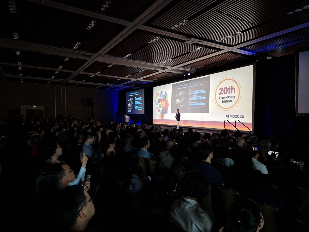
The biggest story in the semiconductor industry last week was FMS (Future of Memory and Storage) 2026. Samsung Electronics and SK hynix — the world's top two memory chip makers — competed to unveil next-generation technologies aimed at the AI era.
FMS, held annually in Santa Clara, California, was not always the broad memory technology showcase it is today. The event launched in 2006 under the name Flash Memory Summit. Starting in 2024, as the rise of AI and high-performance computing blurred the lines between DRAM and next-generation memory and storage technologies, the conference rebranded under its current name.
A shared memory reservoir to ease AI inference bottlenecks as KV cache demand surges
The topic that dominated presentations from both Samsung Electronics and SK hynix at FMS 2026 this year was CXL (Compute Express Link), widely described as the next-generation HBM.
CXL remains an unfamiliar term to many. As the word "link" suggests, it centers on connectivity — a technology that connects CPUs, GPUs and memory chips to push past the limits of bandwidth and capacity.
As AI moves beyond simple learning tasks into the era of large language model (LLM) inference — where models must understand long contexts — demand for KV cache (Key Value Cache) is surging. LLM-based AI agents temporarily store prior conversation history in KV cache to speed up inference, and as conversations grow longer and user counts rise, KV cache memory requirements can balloon to hundreds of gigabytes.
Because conventional memory alone cannot meet that capacity demand, the idea is to use large-scale CXL memory as a shared reservoir through memory pooling. Once a CXL network is in place, successive generations of the technology could eventually enable a memory reservoir measured in petabytes.
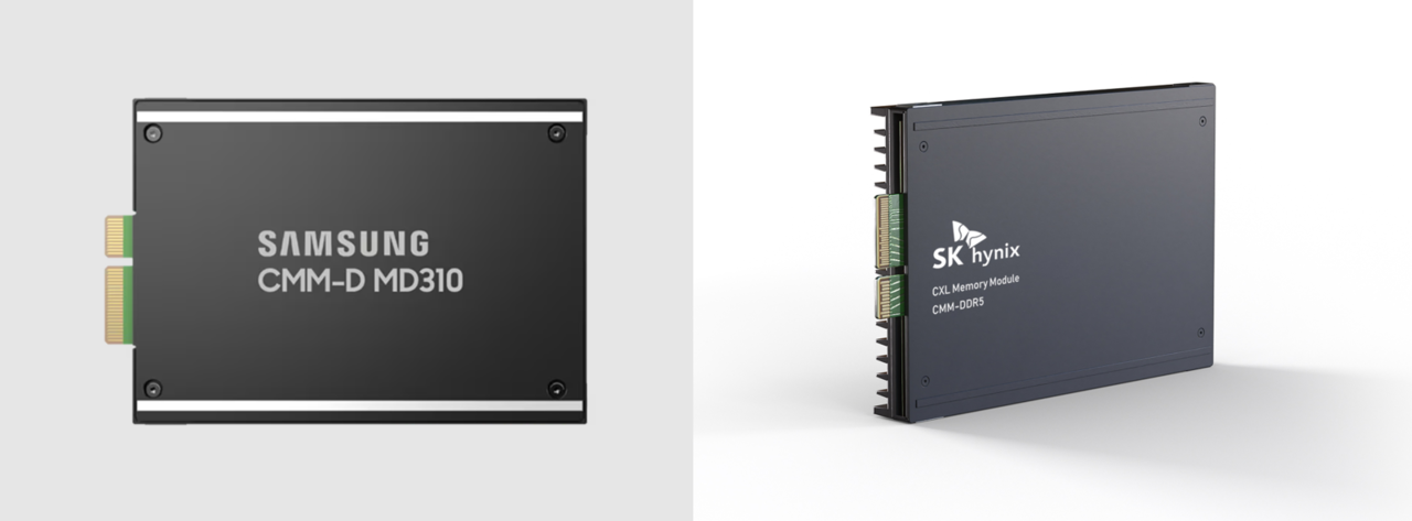
Both companies are deep in development. Samsung Electronics became the first in the industry to develop CXL-based DRAM technology in 2021, and SK hynix followed the very next year with its own CXL memory samples.
Both have also recently presented results from applying CXL technology to LLM inference. Samsung Electronics released findings from a "CXL memory pooling-based KV cache offloading" experiment: in a 512GB DRAM configuration, KV cache demand exceeded available memory capacity and performance degraded, while a 1TB CXL memory pool sustained KV cache demand and kept performance stable.
SK hynix, working with Marvell, unveiled CMM-Ax — a CXL-based PNM (Processing-Near-Memory) module — earlier this month. By having the memory handle computation as well, the module achieved throughput up to 5.5 times higher than a single GPU and 3.6 times higher than a dual-GPU setup in ultra-long-context LLM environments. The validation was conducted with 512GB of capacity per device.
Nvidia's dominant ecosystem creates headwinds — but 'AI agent solutions' are rising
If the world's two largest memory chip makers are both pushing CXL, why does the technology still feel unfamiliar? The answer involves a key industry player with little interest in seeing CXL spread: Nvidia.
Nvidia connects GPUs and CPUs through its proprietary NVLink standard. Now in its sixth generation, NVLink supports 3.6 terabytes per second of bandwidth per GPU, enabling tens to hundreds of GPUs in Blackwell- and Rubin-based data centers to work together like a high-performance supercomputer.

Nvidia's strength in the AI data center market lies in locking customers into its ecosystem on the back of dominant GPU performance. The company has built an exclusive programming ecosystem around CUDA, its proprietary parallel computing platform. The spread of CXL — an open interconnect standard — would inevitably affect Nvidia's position.
The companies driving CXL also help explain Nvidia's reluctance. Intel launched the CXL consortium in 2019 to expand the ecosystem around its Xeon data center CPUs, drawing in global cloud hyperscalers and memory companies. Nvidia has joined the consortium — largely to monitor future customer demand and keep a check on the ecosystem — but its enthusiasm for the standard remains limited.

There are those who push back on that skepticism, however, arguing that the momentum toward CXL is too strong to resist. FMS 2026 featured presentations making exactly that case.
So Jin-in, senior director of memory system architecture at Samsung Electronics, and Lee Ho-gyun, director of DRAM solution engineering at Samsung Electronics, made that argument Thursday (local time) in a presentation titled "The Revival of CXL in the AI Era," directly referencing NVLink.
"A few years ago, some industry reports claimed that CXL was finished in the AI era, citing bandwidth limitations compared with interconnects like NVLink," the two said. "CXL is now emerging as a core solution by leveraging its low-latency characteristics alongside large-capacity memory pooling and sharing technology."
Adding compute to memory to target the on-device AI market
Beyond CXL, both companies showcased another next-generation technology at FMS 2026: PIM (Processing-In-Memory), which enables memory chips to perform computation in addition to storage — a role memory has traditionally not played.
The spread of agentic AI and LLMs has sharply increased the need to process data quickly. In conventional computer architecture, the processor handling computation and the memory storing data have always been physically separate.
By designing computational circuits inside the storage cells themselves, however, memory can handle basic operations on its own. This reduces the amount of data moving between components, boosting speed and cutting power consumption.
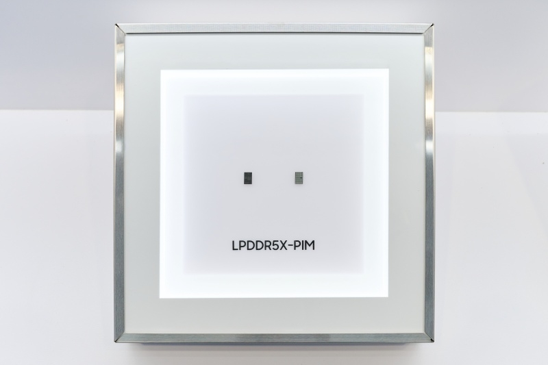
Samsung Electronics brought its LPDDR5X-PIM (low-power DRAM with PIM) to FMS 2026 — the world's first such device — combining low-power DRAM with PIM technology. The product won the FMS Best of Show Award. SK hynix also used the conference to outline its development roadmap for LPDDR6-PIM.
Why are both companies working to embed data processing into LPDDR chips? The technology targets the edge AI market — devices such as on-device AI that operate without routing through a central cloud server. Because the memory handles computation itself, high-performance AI can run at low power even without large servers.
Combining PIM with CXL is another technical challenge both companies face. SK hynix's CMM-Ax, mentioned earlier in the context of CXL, stops short of full PIM but performs computation close to the memory, amplifying the synergy. In CMM-Ax, 16 CPUs embedded in Marvell's CXL controller handle the processing.
Stacking race extends to NAND — SK hynix's HBF vs. Samsung's zNAND-O
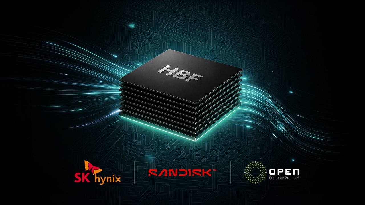
The discussion so far has focused on DRAM, but a notable NAND development also emerged at FMS 2026. By far the most attention-grabbing NAND technology at the show was HBF (High Bandwidth Flash). SK hynix — which leads the HBM market by share — joined with SanDisk to publish the first formal HBF standard specification, covering capacity, bandwidth and connectivity, effectively signaling to the industry what the format will look like and inviting others to build to it.
The idea is that a new tier like HBF needs to sit within the existing hierarchy — GPU HBM, DRAM and SSDs (solid-state drives) — to provide additional capacity. Stacking NAND the way HBM stacks DRAM, while retaining data even when power is cut, means HBF can offer far greater capacity than DRAM at a relatively lower cost.
Samsung Electronics did not make a separate HBF announcement — but that does not mean it is sitting out the race.
Samsung presented its 3D memory architecture vision under the name "zNAND-O," a technology that uses TSV (through-silicon vias) to stack four or eight semiconductor chips in a 3D package. Where conventional stacked structures route data through wires running along the chip's outer edges, zNAND-O shortens the transmission path by routing signals through internal electrodes, improving both speed and power efficiency.
Both Samsung Electronics and SK hynix are pursuing the same fundamental concept — stacking NAND vertically — but under different names, a rivalry that reflects the pride of two memory giants. The industry expects HBF technology to reach commercial deployment around 2030.
jeongwan@heraldcorp.com