Joins ASML-led consortium for 12-inch photomask standard
Partnership targets shift from current 6-inch masks
High-NA EUV adoption aims to boost DRAM miniaturization, productivity
Next-generation lithography to extend from foundry to advanced memory

Samsung Electronics will join the Large Size Mask Consortium led by Dutch lithography equipment maker ASML to jointly develop next-generation 12-inch photomasks.
The company expects the move to lower chip production costs and boost productivity. Samsung also plans to become the first in the industry to introduce ASML's next-generation lithography tool — High-NA extreme ultraviolet (EUV) equipment — into advanced DRAM production by 2028.
Lithography equipment is used in the semiconductor process to etch circuit patterns onto wafers using light. ASML's High-NA EUV tools draw finer circuits than existing equipment, making them essential for achieving greater miniaturization.
According to Samsung on Tuesday, the ASML-led Large Size Mask Consortium aims to shift the photomasks used in lithography equipment from 6 inches to 12 inches.
A photomask is a precision template etched with microscopic circuit patterns. It is an essential tool for transferring designed patterns onto wafers using light inside lithography equipment. The higher the precision of the etched circuits, the greater the improvement in chip performance and yield.
Lithography processes have long relied on 6-inch masks. But switching to 12-inch masks alongside the adoption of High-NA EUV would eliminate the constraints of stitching — the process of etching patterns in sections and joining them together — boosting fab productivity and lowering chip manufacturing costs.
This is particularly true for advanced chips that require precise placement of hundreds of billions of transistors at the design stage. Twelve-inch masks would allow full use of the benefits of High-NA EUV equipment, enabling more economical production.
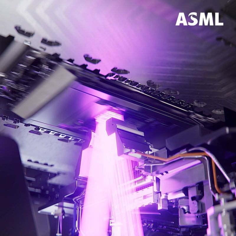
Through its participation in the consortium, Samsung plans to monitor global technology trends related to lithography equipment and photomasks, while cooperating on joint research and standard development aimed at 12-inch photomasks.
Given its long experience with EUV and its technological leadership, Samsung is expected to play a key role in the shift to 12-inch photomasks.
Samsung also said it is pushing to introduce High-NA EUV into advanced DRAM memory chip manufacturing by 2028. This signals that it is preparing to apply the next-generation lithography equipment to advanced memory chips, following its use in foundry processes.
High-NA EUV draws circuits with greater precision, which is expected to extend Samsung's roadmap for DRAM miniaturization while contributing to process simplification and higher productivity. ASML, the world's sole producer of High-NA EUV equipment, is often called the semiconductor industry's "super-supplier."
As circuit line widths narrow, more circuits can be drawn on a single wafer, increasing the number of chips that can be produced. Narrower line widths also enable faster computation and lower power consumption.
Building on their years of cooperation, Samsung and ASML plan to accelerate the development and adoption of new technology. The goal is to raise the performance and efficiency required for advanced AI chip manufacturing.
"The arrival of the AI era is transforming the semiconductor industry's paradigm and further heightening the importance of technological innovation across the value chain," said Jun Young-hyun, vice chairman and CEO of Samsung Electronics. "Samsung Electronics will continue its leadership in advanced semiconductor manufacturing, including foundry and memory chips, and will further strengthen its cooperation with ASML to build the technological foundation for 'Next AI.'"
ASML CEO Christophe Fouquet said, "Samsung Electronics has long been one of ASML's most important innovation partners, and together we have advanced the technologies that underpin modern semiconductor manufacturing. As we enter a new era led by AI, we look forward to driving innovation together with Samsung Electronics for next-generation semiconductor manufacturing."
The two companies plan to explore further cooperation opportunities in advanced memory chips and innovative manufacturing methods going forward.
joze@heraldcorp.com