Show opens Wednesday at COEX in Gangnam-gu, Seoul
HBM4E samples already shipped to Nvidia put on public display
Samsung shows zHBM, zNAND-O mockups
SK hynix highlights HBF as solution to inference bottleneck
Samsung also outlines Yongin industrial complex investment plan
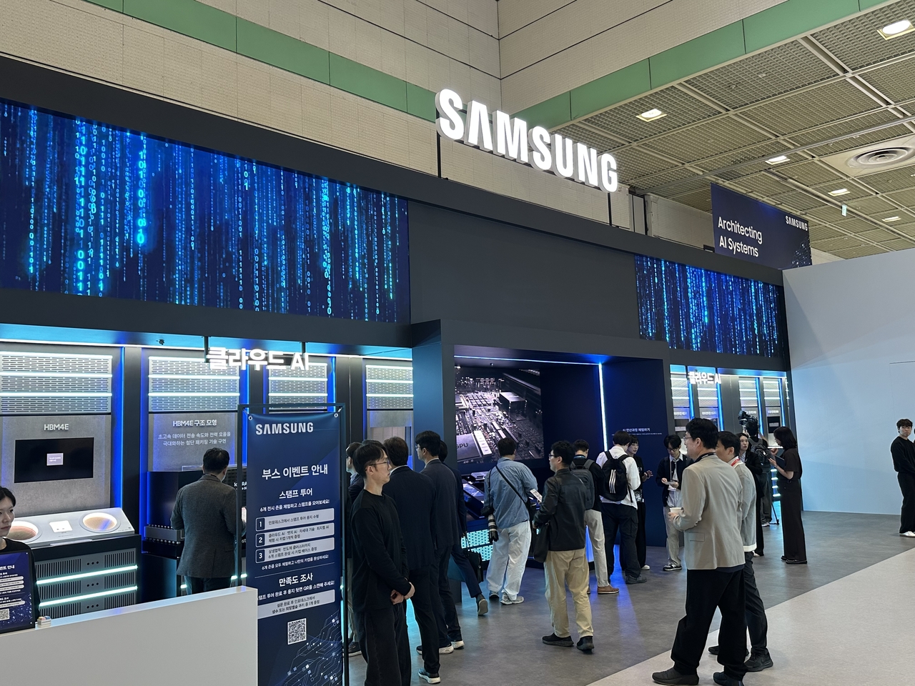
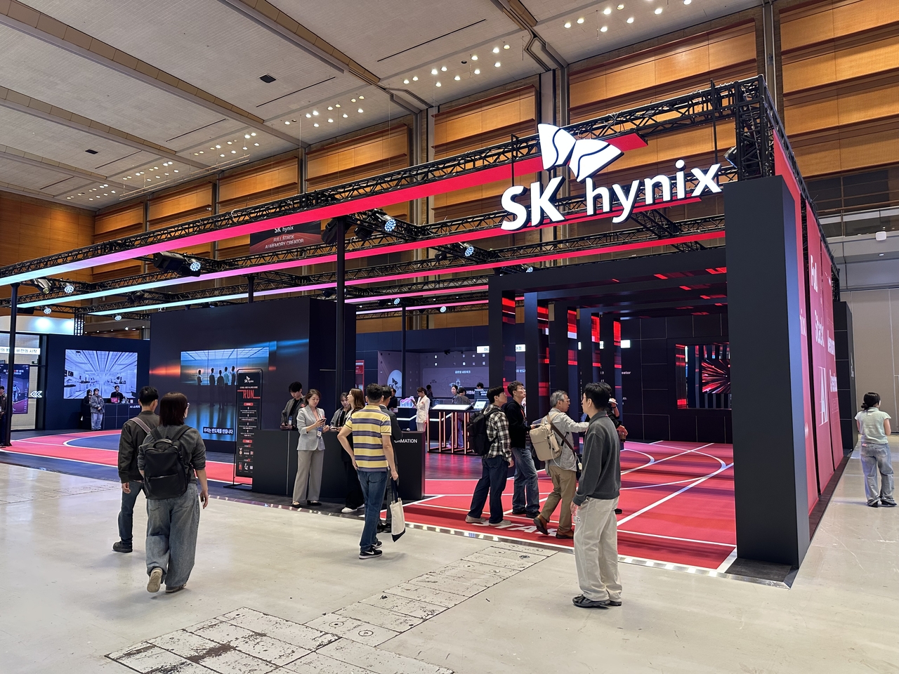
Samsung Electronics and SK hynix unveiled their latest AI-focused memory chip technologies Wednesday at the 28th Korea Semiconductor Exhibition, known as SEDEX 2026. Both companies put physical samples of their seventh-generation high-bandwidth memory, HBM4E, on display, signaling that competition in the HBM space will only intensify.
Each company also introduced its own future memory solution aimed at eliminating computational bottlenecks. Samsung Electronics showed a mockup of zHBM, which stacks HBM vertically on top of a GPU, while SK hynix promoted its HBF — high-bandwidth flash — technology as a new layer in the memory hierarchy.
The exhibition, organized by the Korea Semiconductor Industry Association, runs through Friday at COEX in Gangnam-gu, Seoul. It is the country's largest dedicated semiconductor trade show, drawing more than 300 companies spanning memory chips, system semiconductors, materials, components and equipment.
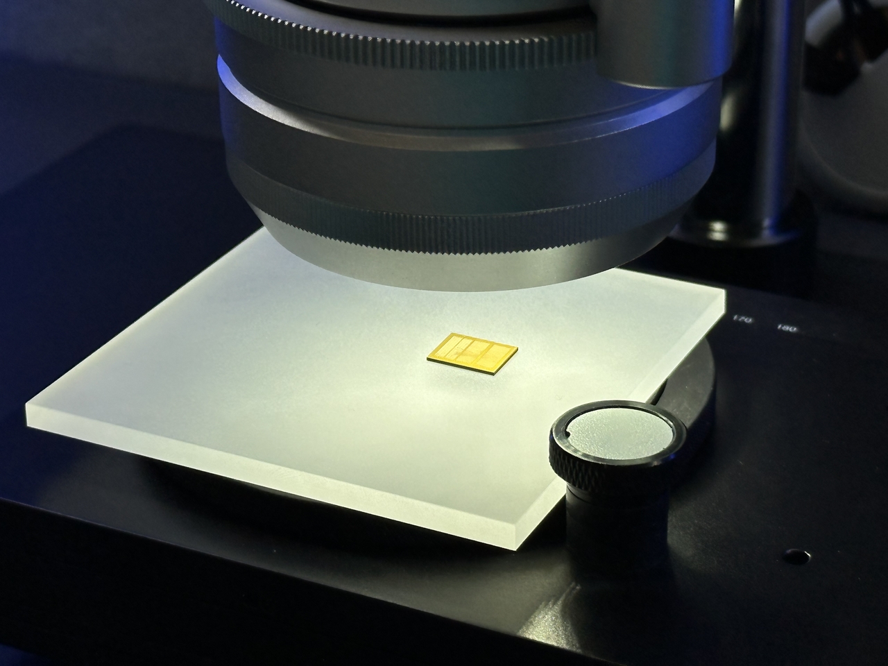
Both companies placed HBM front and center in their exhibition halls. Demand for HBM produced by the two global memory chip leaders has surged as investment in AI data centers continues to expand.
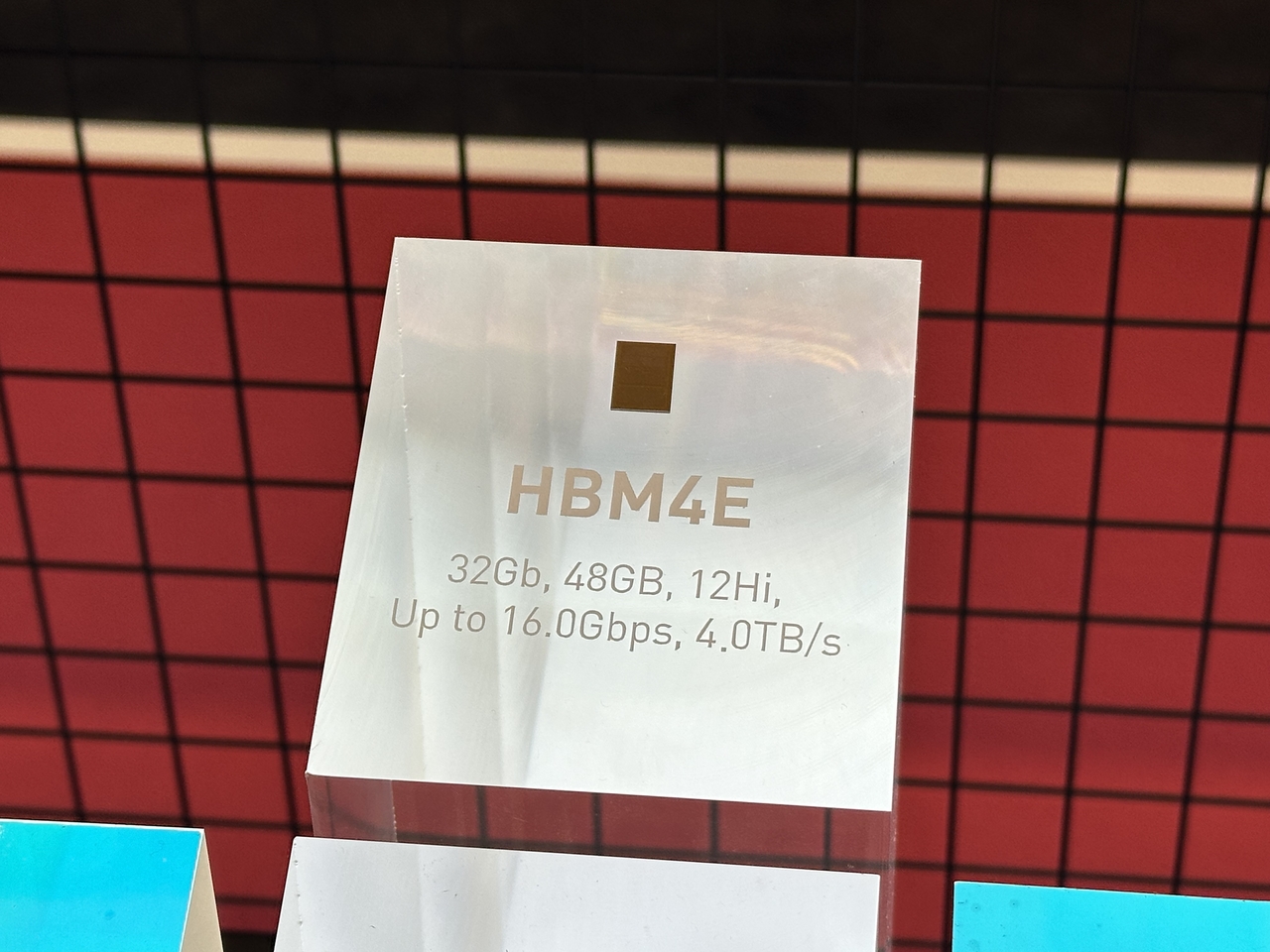
HBM4E, the next-generation HBM, drew particular attention from visitors. Samsung Electronics shipped 12-layer HBM4E samples to Nvidia in May, and SK hynix followed in June.
Samsung Electronics' HBM4E operates at up to 16 gigabits per second per pin — a 20 percent improvement over HBM4 from a baseline of 14 Gbps — and delivers 3.6 terabytes per second of bandwidth to maximize processing speed. SK hynix's HBM4E also achieves a peak data transfer rate of 16 Gbps while improving energy efficiency by more than 20 percent compared with its predecessor.
Both companies also showcased the future memory architectures they are developing. Samsung Electronics placed at the front of its booth a mockup of zHBM — a 3D memory architecture first revealed at FMS (Future of Memory and Storage) 2026 in Santa Clara, California, in August — alongside a mockup of zNAND-O, a 3D NAND solution optimized for edge AI. By shortening the distance data must travel between the GPU and memory, zHBM is designed to support the ultra-fast data processing required for training and running large AI models.
SK hynix similarly showcased the HBF architecture it introduced at FMS 2026. The company proposes adding HBF as a new tier alongside the existing memory and storage stack — which currently comprises HBM, server DRAM and SSDs — as a solution to inference bottlenecks. HBF offers bandwidth comparable to HBM and capacity comparable to NAND flash, enabling higher computational throughput at a relatively lower price. SK hynix has already published a standard specification for the technology together with SanDisk.
Samsung Electronics also highlighted its foundry business alongside its memory offerings, emphasizing its base-die production capabilities — widely cited as a key advantage in the era of custom HBM. The company presented an HBM4E base die manufactured on a 4-nanometer process. Integrating advanced foundry logic with HBM, it said, can deliver benefits in system performance, power efficiency and design flexibility.
Samsung Electronics also outlined its strategy for expanding production capacity to meet surging demand, introducing the roles of its key manufacturing and development sites and presenting plans for the Yongin national industrial complex.
Samsung Electronics plans to invest about 360 trillion won ($269 billion) in the Yongin complex. It aims to begin site preparation and break ground next year, with the first production line targeted to begin operation in October 2029. About 70 materials, components, equipment and fabless companies are expected to move into the complex.
jeongwan@heraldcorp.com