- DGIST and Yonsei University identify optical response mechanism in ultrathin silicon films
- Findings expected to advance next-generation nondestructive testing for flexible and 3D semiconductors

A team of Korean researchers has found a way to analyze microscopic wrinkles on semiconductor surfaces thousands of times thinner than a human hair — using light alone, without damaging the material.
The Daegu Gyeongbuk Institute of Science and Technology announced Monday that a team led by Professor Lee Jae-dong of its Department of Chemistry and Physics and Senior Researcher Kim Hyun-min of its Biomedical Research Institute, working jointly with a team led by Professor Ahn Jong-hyun of Yonsei University's School of Electrical and Electronic Engineering, had identified the optical response mechanism of wrinkled ultrathin silicon films.
Silicon is the core material used to make semiconductors. When its thickness is reduced to tens of nanometers (nm, or one-billionth of a meter) or less, it becomes flexible enough to bend freely, making it suitable for next-generation flexible electronic and photonic devices.
The challenge is that as silicon films grow thinner, even tiny wrinkles can significantly alter the material's properties. The degree to which silicon stretches or compresses differs between the peaks and valleys of a wrinkle, causing its optical response to change in complex ways.
Such microscopic deformations are directly tied to semiconductor performance, but existing analytical methods have struggled to measure them accurately.
To address this, the research team combined third-harmonic generation (THG) microscopy — which produces new light by tripling the frequency of an input beam — with first-principles calculations based on quantum mechanics.
The Yonsei University team fabricated wrinkled silicon nanomembranes using precision processing, while the DGIST team irradiated them with infrared light at a wavelength of 1,040 nm.
As a result, resonance between electrons inside the silicon and the light generated a strong ultraviolet signal at a wavelength of approximately 346 nm.
When the team analyzed this signal, they found that the ratio of signal intensity according to the polarization direction of light differed markedly between the peaks and valleys of the wrinkles.
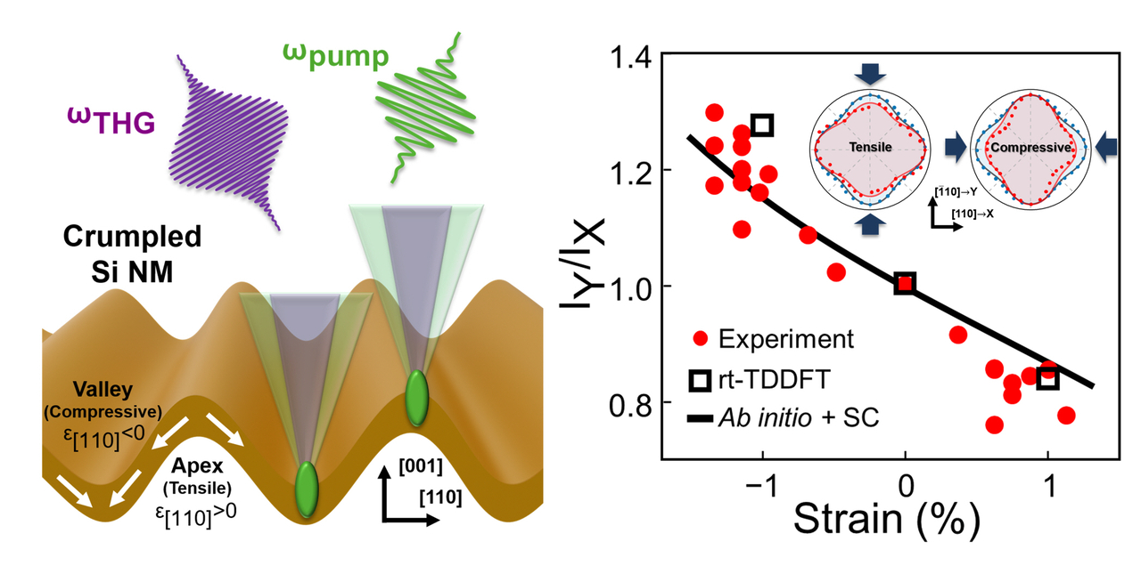
A new phenomenon emerged when the silicon film was thinned to around 15 nm.
At that thickness, not only did the electronic structure inside the silicon change, but the three-dimensional shape of the wrinkled surface itself began to alter the distribution of surrounding light, exerting a significant influence on the optical signal.
The team incorporated the light distribution around the wrinkles into their calculations through electromagnetic field simulations, and confirmed that the experimental results matched their theoretical predictions.
The findings are expected to contribute to the development of next-generation nondestructive testing technology capable of analyzing the internal deformation of semiconductors without cutting or damaging them.
The research is particularly expected to enable precise analysis of microscopic deformations in flexible displays, flexible electronic devices and complex three-dimensional semiconductor structures, and to help predict device performance.
However, applying the technique to actual semiconductor manufacturing processes will require improvements in the precision and speed of optical measurement equipment, as well as additional verification for complex three-dimensional device structures.
"We expect this to develop into a next-generation nondestructive testing technology that can precisely diagnose strain in three-dimensional semiconductor structures without damaging the material," Lee said.
The findings were published in the international journal Nano Letters.
nbgkoo@heraldcorp.com