- National NanoFab Center successfully test-fabricates silicon bridge for advanced packaging
- Integrates 1-micrometer copper wiring and through-silicon vias, with 12-inch process expansion planned
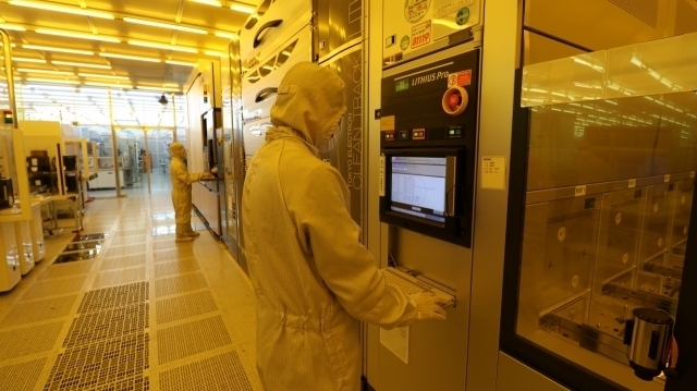
South Korean researchers have developed a key technology that enables faster and denser connections between the multiple chips that make up AI semiconductors.
The National NanoFab Center announced Wednesday that a research team led by Kang Il-seok, director of its Advanced Packaging Development Center, and Senior Researcher Jang Hee-jun had secured silicon bridge process technology capable of high-speed data transfer and high-density interconnection between chiplets. It marks the first time a silicon bridge has been test-fabricated at a public nanofab facility in South Korea.
AI semiconductors have increasingly moved away from integrating all functions into a single large chip, instead adopting a "chiplet" approach that bundles together smaller chips divided by function — such as processing and memory chip. The shift allows chipmakers to boost performance while improving manufacturing efficiency.
The challenge lies in the connections between chiplets. No matter how capable individual chips are, slow data transfer between them inevitably drags down overall semiconductor performance.
Silicon bridge technology addresses that limitation. It works by placing a small silicon piece between chips and embedding ultrafine wiring within it to create a data pathway, allowing high-density interconnects to be concentrated precisely where they are needed.
The technology is already used in advanced packaging solutions such as CoWoS-L and EMIB by global chipmakers, and its applications are expanding into large-area panel-based packaging and co-packaged optics (CPO), which integrates electronic circuits and photonic devices.
The research team successfully stacked multiple layers of copper wiring on an 8-inch silicon wafer, with both line width and spacing of approximately 1 micrometer (one-millionth of a meter).
The team also implemented through-silicon vias (TSVs) — a technique that drills microscopic holes through silicon and fills them with copper to create vertical electrical connections between layers.
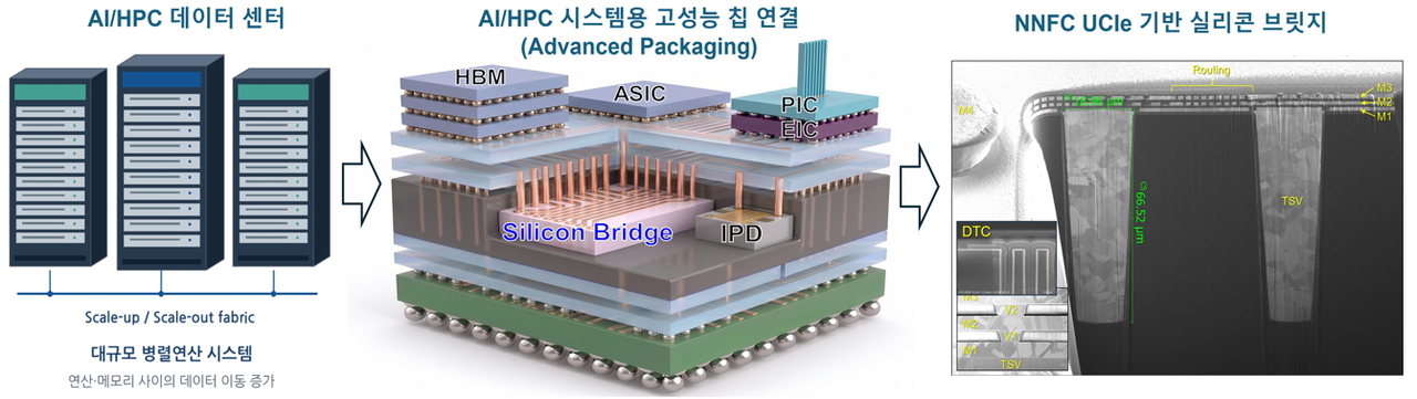
The structure enables not only horizontal connections between chiplets but also vertical electrical links. Capacitors for stable power supply and copper bonding bumps were also integrated into the design.
The design incorporates the UCIe international standard, which allows chiplets made by different companies to be interconnected.
The significance of the achievement lies in establishing a foundation for test-fabricating and validating advanced packaging technology at a domestic public research facility.
Silicon bridge technology, previously the domain of global chipmakers, will now be accessible to South Korean researchers in industry, academia and government institutes through the public nanofab infrastructure.
The National NanoFab Center has been building a 300-millimeter (12-inch) advanced packaging infrastructure with support from the Ministry of Science and ICT since 2024. It is currently acquiring more than 20 key pieces of equipment in stages, with plans to expand the technology to a 12-inch wafer-based silicon bridge process.
The center aims to support the full cycle — from test fabrication to performance verification — of advanced packaging technology needed for next-generation AI semiconductors and high-performance chips.
"This achievement is meaningful in that it has laid the groundwork for public nanofab support for domestic researchers in industry, academia and government to develop and commercialize core advanced packaging technologies," National NanoFab Center President Park Heung-su said. "We will continue to advance our open infrastructure and process technology to broaden opportunities for demonstrating advanced packaging capabilities in South Korea."
The findings were presented Wednesday at the 24th International Symposium on Microelectronics and Packaging (ISMP 2026).
nbgkoo@heraldcorp.com